
Polycrystals
Organic Semiconductors have emerged as crucial materials in the development of electronic and optoelectronic devices due to their exceptional mechanical flexibility, lightweight nature, and cost effectiveness. Charge carrier mobility is one key quantity to measure the performance of OSC devices. Our study uses Non-Adiabatic Molecular Dynamics (NAMD) simulations, employing Fewest Switches Surface Hopping (FSSH) approach to model charge transport dynamics. The charge transfer Hamiltonian was constructed using a fragment orbital approach, with its elements computed via the Density Functional Tight Binding (DFTB) method.
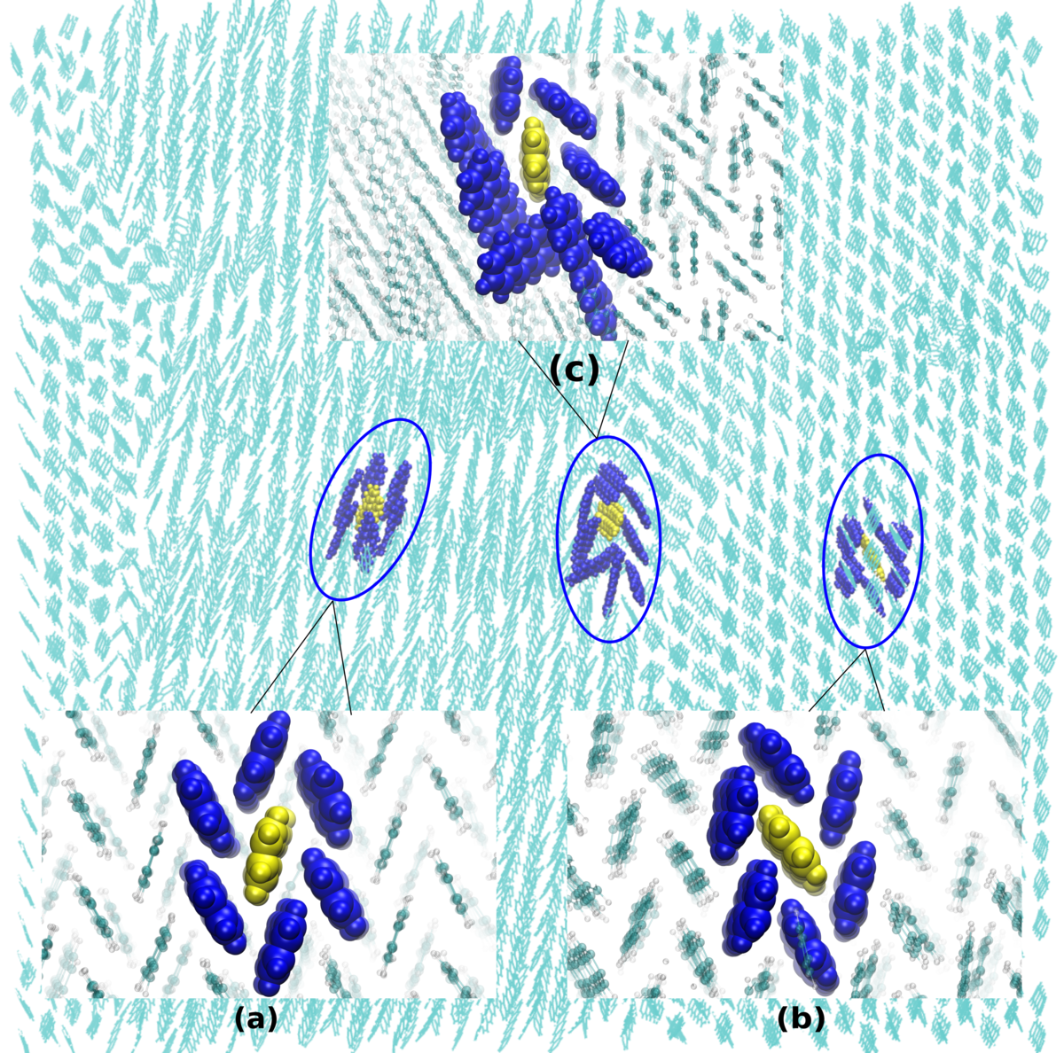
In previous projects, we examined intrinsic charge carrier mobility in ideal single crystals of small organic molecules such as pentacene, rubrene, anthracene, and DATT, achieving results comparable to experimental findings. However, for more complex molecular systems, deviations from experimental mobilities suggest the need to account for thin-film effects. Current research explores the impact of grain boundaries (GBs)—a critical feature in polycrystalline OSC thin films. GBs can act as traps or barriers, hindering charge transport and reducing device efficiency. By analyzing how factors like misorientation angles and grain boundary width affect charge carrier mobility, we aim to bridge the gap between intrinsic and device-level mobilities, contributing valuable insights toward the optimization of OSC-based devices.
